Posted on 17-Mar-2017 20:02
Views 591
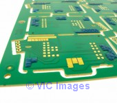
Via in Pad PCB Manufacturer - Via In Pad is plated through Hole filled with conductive (or non-conductive) epoxy plugging ink, subsequently planar zed and plated over. Via-in-Pads are usually patterned into a BGA pad for direct soldering. Via In Pad PCB, No of Layer: 4, 6 or more, Material: FR-4, TG170, KB/Shengyi, Board thickness: 1.6mm, Copper weight: 35um=1oz, Surface finishing: ENIG=Immersion Gold, Solder mask: Glossy Blue, Silk screen: White, Key technology: For more details go with - www.jps-pcb.com/products/multi-layer-pcb/via-in-pad-pcb.html
Address www.jps-pcb.com Building 2, Tongfuyu Industrial Park, Shenzhen, China, 518104 Baggio +86-755-82596922 8 Layer Impedance PCB, 2W thermal Aluminum PCB, Copper based PCB, impedance control PCB, 2 layer aluminum PCB, blind via PCB, buried via PCB, 10 Layer PCB, rigid-Flex PCB